If you’ve ever worked on a high-frequency high-voltage rectifier PCB, you know the pain of noise creep. That high-pitched whine from the transformer, random voltage spikes messing with your control loop, or signal integrity errors that pop up right when you think you’ve got the design nailed? I’ve been there—10 years as a PCB supplier specializing in high-frequency high-voltage rectifiers, and I’ve lost count of how many clients come to me with designs that worked on a breadboard but turned into a nightmare once sent to fab. The problem almost never is the rectifier itself; it’s the small, avoidable noise culprits on the PCB layout. PCB High Frequency High Voltage Rectifier
Let’s break this down, no jargon overload, just what actually works for real boards, not just textbook theory. First, let’s get clear on what noise we’re dealing with here. High-frequency rectifiers (think 100kHz to 1MHz, not the 50Hz wall plug variety) switch really fast—like, nanoseconds fast. Every time the diode turns on or off, you get a current spike, and if that spike can loop around easily, it creates electromagnetic interference (EMI) that turns into both radiated noise and conducted noise. Worse, high voltage amplifies this: a 10A current spike at 500V doesn’t just create a small buzz—it can mess with adjacent low-voltage circuits, cause component overheating, or even trigger false fault codes.
The first mistake most people make is placing the key components wrong. Your rectifier diodes, the input filter caps, and the transformer secondary windings—they need to form what’s called a “low-inductance loop” for the switching current. Inductance is the enemy here because it resists current changes, so a tight loop (the shorter the better) means less inductance, less spike, less noise. I see designers spread these parts across the board to “save space” or fit other components, but that loop length doubles or triples, and noise skyrockets. Rule of thumb: tuck your high-voltage diodes, input bulk cap, and transformer terminals right next to each other on the same layer, no vias in that loop if you can help it. If you have to use a via, make it a stacked via pair for the high-current path—stacked vias reduce inductance way more than a single via.
Next up, decoupling caps—wait, not the small ceramic ones for low-voltage logic, the right bulk caps for your rectifier. A lot of designers use electrolytic caps here because they’re cheap and high capacitance, but electrolytics have bad high-frequency performance—their equivalent series resistance (ESR) and equivalent series inductance (ESL) go up at frequencies above 100kHz, so they can’t suppress the fast current spikes. I always tell clients to pair a low-ESR ceramic cap (0.1µF or 1µF, X7R or X5R dielectric) right next to the diode anode and cathode, plus a 10µF polymer electrolytic cap a little further away for lower-frequency noise. The ceramic cap handles the nanosecond spikes, the polymer handles the slower current draw. Also, make sure the cap leads are as short as possible—no bending them around other parts. I’ve seen clients add 1cm of lead here and wonder why their noise went up by 20dB.
Then there’s the ground plane, or lack thereof. For high-frequency high-voltage designs, a solid ground plane is non-negotiable, but not just any ground plane—you have to split it properly, or at least isolate the noisy power ground from the sensitive signal ground. Let’s be real: your rectifier’s switching current is high-voltage, high-frequency, so if that ground is shared with your microcontroller or sensor circuits, the noise will couple into the signals. I recommend a split ground plane, but only separate it once—never separate and rejoin with a via, that creates a huge inductance path. Instead, run a 1cm wide “island” of ground for the signal side, and the main ground plane for the power side, with a single star ground point where they connect. That way, all the noise current stays on the power ground, and the signal ground stays clean. Another tip: don’t run signal traces parallel to high-voltage switching traces. That’s a direct antenna for noise. If you have to cross them, do it at a 90-degree angle, and keep the signal trace as far away as possible—at least twice the trace width.
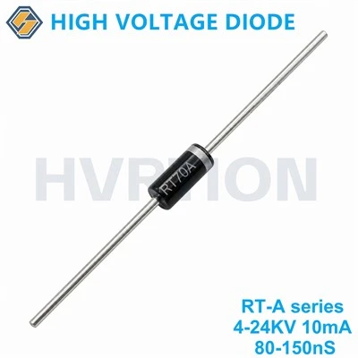
Wait, what about the rectifier diodes themselves? Not all diodes are created equal for high-frequency noise. A standard silicon diode has reverse recovery time—when it turns off, it has a period where it’s still conducting reverse current, which creates a huge spike. For high-frequency designs, you need fast recovery diodes or Schottky diodes with very low reverse recovery time (under 50ns, ideally). I’ve had clients use cheap generic diodes here and wonder why their EMI emissions failed compliance testing right before product launch. It’s a small part cost difference, but it makes a massive impact on noise. Also, add a snubber circuit across the rectifier output, but not just any snubber—use a small capacitor (1nF to 10nF) in series with a resistor (10Ω to 100Ω), not just a resistor or just a capacitor. Too big and you add power loss, too small and it doesn’t dampen the spikes. I usually tune this on the lab bench for each design, since transformer inductance and switching frequency change things.
Routing details are where most noise gets missed. Traces for high-current rectifier paths should be wide enough to keep current density low, but also, keep them short. If your trace is 5cm long instead of 1cm, that’s 5x more inductance. Also, avoid right-angle turns on high-voltage traces—90-degree turns create a discontinuity that reflects high-frequency signals, leading to more noise. Use 45-degree turns or rounded corners instead. If you have to use a via, make sure it’s in the middle of the trace, not at an edge, and keep the pad for the via as small as possible—smaller pad means less capacitance, which means less noise coupling.
Thermal management might seem unrelated, but hear me out. If your rectifier diodes run hot, their reverse recovery time increases, which leads to more noise. I see clients skimp on thermal vias for power diodes to save space, but a thermal via that connects the diode pad to the ground plane (a thermal relief pad, not a solid pad—solid pads create too much capacitance) keeps the diode cool, which stabilizes its switching performance and reduces noise. Also, make sure there’s enough airflow around the rectifier module, but that’s more mechanical—on the PCB side, thermal vias are a quick fix.
Let’s talk about a real example, not a hypothetical. Last year, a client came to me with a 400V 500kHz rectifier PCB that was failing CISPR 22 EMI testing. Their breadboard worked, but the PCB had 30dB of radiated noise at 500kHz. We went through their design, and the first mistake was the current loop: their diodes were 2cm away from the input cap, with a 3cm trace between them. We moved them within 5mm, added a 0.1µF ceramic cap right next to the diodes, split the ground plane, and changed their standard diodes to fast recovery ones. After a couple of tweaks to the snubber resistor, they passed EMI on the first re-test. The fix took less than 2 hours of layout changes, no new parts, just a few small adjustments.
Common myths to bust here: first, more caps = better. No, adding extra bulk caps without considering ESL will make noise worse, because multiple caps in parallel can have resonant frequencies that amplify noise at certain frequencies. Second, a thicker PCB is always better. No, thickness doesn’t fix noise—design choices (loop length, ground plane, component placement) do. Third, shielding is the only fix. Shielding works, but it’s expensive, adds weight, and can cause grounding issues if not done right. Fixing the root cause on the layout is cheaper and more reliable.
Now, if you’re working on a high-frequency high-voltage rectifier design, don’t guess at these changes. A lot of the time, noise is subtle—you might see it in an oscilloscope trace, but not in a breadboard, because breadboards have way more parasitic inductance and capacitance than you think. That’s where working with a supplier that actually designs and fabricates these PCBs helps: we’ve got the lab equipment to measure noise at every step, so we can catch issues before the board goes to production.
If you’re dealing with persistent noise on your high-frequency rectifier PCB, or you’re designing a new board and want to avoid these headaches before fab, reach out to us to walk through your layout, test your design, or get custom PCB fabrication tailored to your rectifier requirements. We’ve worked with everything from consumer electronics to industrial power supplies, so we know how to get noise under control without cutting corners on performance.
Wait, one last quick tip: after layout, do a noise simulation before ordering the board. A lot of EDA tools (Altium, KiCad, OrCAD) have noise simulation features for high-frequency designs. It takes an hour to run, and it can catch loop length issues or ground plane problems that you’d only see once the board is built. Don’t skip that step—we’ve had clients who ordered a batch of 100 boards only to find noise issues that would’ve been caught with a 1-hour simulation.

At the end of the day, mitigating noise on high-frequency rectifier PCBs is all about minimizing the paths for noise to loop and couple, and picking the right parts and layout techniques for high-speed, high-voltage switching. It’s not about over-engineering—It’s about being intentional with every placement and trace, which saves you time, money, and headache in the long run.
Electrostatic Spray Gun High Voltage Module References
- Application Note AN-1001: "EMI Reduction Techniques for High-Frequency Rectifiers", Texas Instruments, 2021
- High-Voltage PCB Design Guidelines, IPC-2221, 2022
- "Parasitic Effects in High-Frequency Power Electronics Circuits", IEEE Transactions on Power Electronics, Vol. 35, No. 7, 2020
- "Fast Recovery Diode Selection for High-Speed Switching Applications", ON Semiconductor, 2019
- Ground Plane Design for Low-Noise High-Frequency PCBs, Mentor Graphics White Paper, 2018
Anshan HVRTION Electronic Technology Co., Ltd.
As one of the most professional pcb high frequency high voltage rectifier manufacturers and suppliers in China, we’re featured by quality products and good price. Please rest assured to buy discount pcb high frequency high voltage rectifier for sale here and get quotation from our factory. We also accept customized orders.
Address: 17 East Jiefang RD., Tiedong District, Anshan, Liaoning, China.
E-mail: hvrtion@hotmail.com
WebSite: https://www.hvrtion.com/
